SS Stepper Controller v1.1 · WaveForge / StabilityCore · ordered 2026-09-17
5-Axis Level Shifter — Board Map
The clean board. No hand modifications, no flying jumpers, the ESP32 seats directly. Supersedes v1.0, which stays in service as a tester.
The board
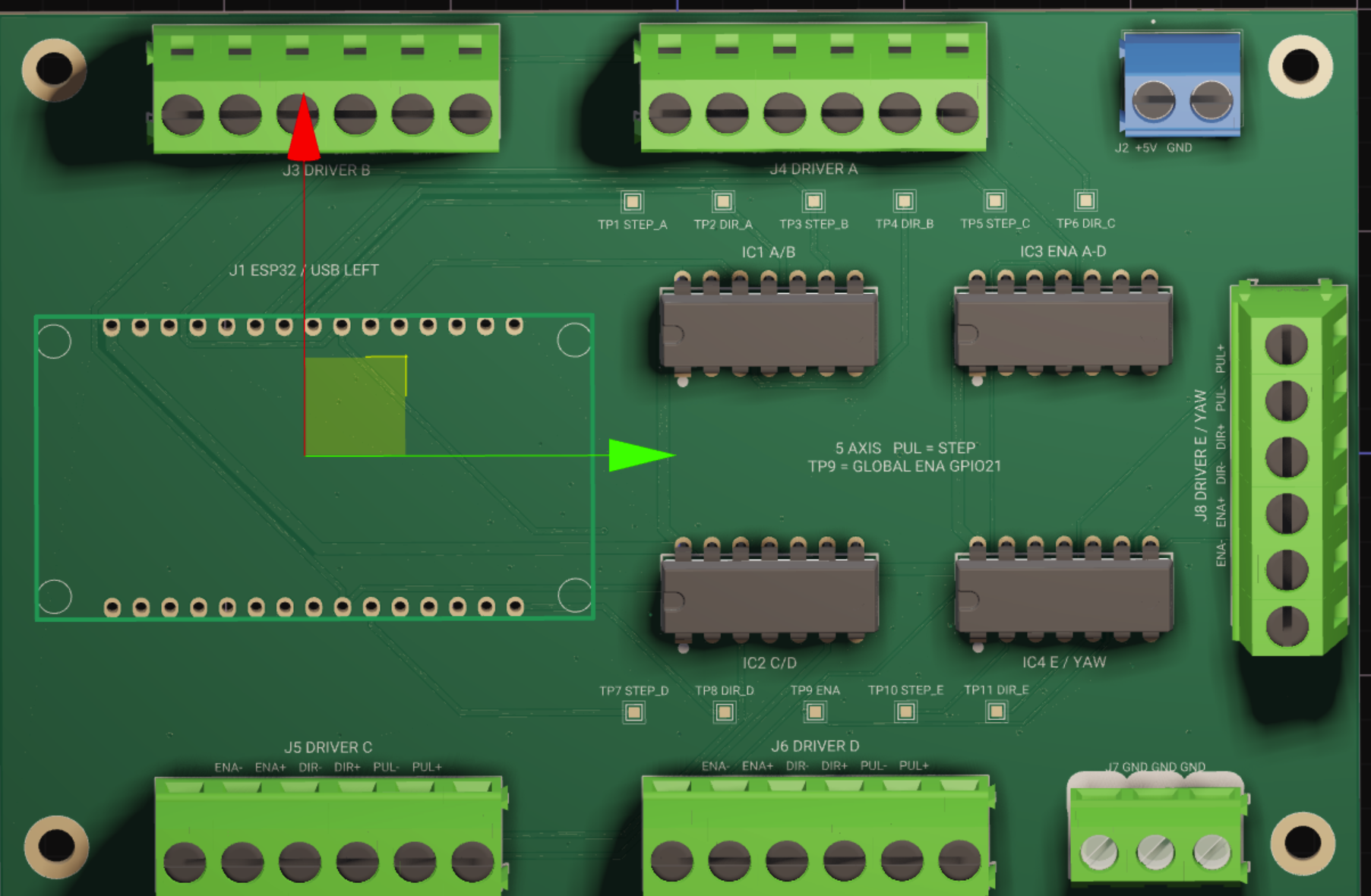
What to read off it before you touch anything:
- The four chip notches all face LEFT. That is the render agreeing with the Gerbers — the rectangular pin 1 pad sits at each socket’s bottom-left. Two independent methods, same answer.
- The terminals ARE labeled, even though they have no pin 1 pad:
ENA− ENA+ DIR− DIR+ PUL− PUL+reading left to right on J5 and J6. That silkscreen is the orientation cue for all five driver blocks. - Eleven test points in two rows. Top: TP1 STEP_A, TP2 DIR_A, TP3 STEP_B, TP4 DIR_B,
TP5 STEP_C, TP6 DIR_C. Bottom: TP7 STEP_D, TP8 DIR_D, TP9 ENA, TP10 STEP_E,
TP11 DIR_E. The board says it plainly:
TP9 = GLOBAL ENA GPIO21. - Chip roles are on the silkscreen too — IC1 A/B and IC2 C/D for step and direction,
IC3 ENA A–D, IC4 E/YAW. And
5 AXIS PUL = STEP, which is the one piece of translation you need when reading a DM542T datasheet. - J1 says
ESP32 / USB LEFTand nothing else. It is the only part with no pad marker at all, so that text is doing the entire job. See the orientation checks below.
Connectors
| Ref | What | Positions | Drill |
|---|---|---|---|
| J1 | ESP32 DevKit, 30-pin, USB to the left | 2×15 @ 2.54 mm, rows 25.4 mm | 1.0 mm |
| J2 | Power in — +5V and GND | 2 @ 5.08 mm | 1.5 mm |
| J3 | Driver B | 6 @ 5.08 mm — PUL+ PUL− DIR+ DIR− ENA+ ENA− | 1.5 mm |
| J4 | Driver A | ||
| J5 | Driver C | ||
| J6 | Driver D | ||
| J8 | Driver E — yaw (new in v1.1) | ||
| J7 | Bench ground | 3 @ 5.08 mm, all GND | 1.5 mm |
ESP32 pin assignment
| GPIO | Signal | Buffer | Terminal | Test pt |
|---|---|---|---|---|
| 25 | STEP A | IC1 A/B | J4 PUL+ | TP1 |
| 26 | DIR A | J4 DIR+ | TP2 | |
| 27 | STEP B | J3 PUL+ | TP3 | |
| 32 | DIR B | J3 DIR+ | TP4 | |
| 33 | STEP C | IC2 C/D | J5 PUL+ | TP5 |
| 18 | DIR C | J5 DIR+ | TP6 | |
| 19 | STEP D | J6 PUL+ | TP7 | |
| 23 | DIR D | J6 DIR+ | TP8 | |
| 14 | STEP E — yaw | IC4 E/yaw | J8 PUL+ | TP10 |
| 13 | DIR E — yaw | J8 DIR+ | TP11 | |
| 21 | ENABLE, all five | IC3 ×4 + IC4 ×1 | every ENA+ | TP9 |
Buffers and passives
| Ref | Part | Channels used |
|---|---|---|
| IC1 | SN74AHCT125N | 4 — STEP/DIR A and B |
| IC2 | SN74AHCT125N | 4 — STEP/DIR C and D |
| IC3 | SN74AHCT125N | 4 — ENA A, B, C, D |
| IC4 | SN74AHCT125N | 3 — STEP E, DIR E, ENA E (1 spare) |
| R1–R11 | 1 k 0805 | pull-down, one per buffer-input net |
| C1–C4 | 0.1 µF 0805 | decoupling, pins 14–7, one per chip |
Pin 1 markers — what this board has and what it doesn’t
From the Gerber apertures, 2026-09-17. This is the copper, not the render.
| Part | Pads | Pin 1 marker? | What that means on the bench |
|---|---|---|---|
| IC1–IC4 sockets | 13 oval + 1 rect each | ✅ yes — rectangular pad, bottom-left | Notch LEFT. Count 1→7 right along the bottom, 8→14 left along the top. |
| J2 power in | 1 round + 1 rect | ✅ yes | Square pad is pin 1. |
| 3-pin connector | 2 round + 1 rect | ✅ yes | Square pad is pin 1. |
| J1 ESP32 header | 30 identical ovals | ❌ none | The silkscreen “USB LEFT” is the only orientation cue. Run the continuity checks below before seating a module. |
| J3–J6, J8 terminals | 30 identical 2.3 mm rounds | ❌ none | No pin 1 anywhere on the five 6-pin blocks. Go by the silkscreen labels and confirm by tracing. |
Assembly order
- Measure a terminal header pin first. Holes are 1.5 mm; the pluggable Phoenix-style part must clear that, and there must be nothing under the header but six pins in a line.
- Underside passives before anything else — R1–R11 and C1–C4 are on the bottom and get awkward once tall parts are on the top.
- DIP sockets, four of them. Orient by the board silkscreen notch.
- J1 headers — two single-row 1×15 female strips, not a dual-row part. Push both onto the ESP32's pins first so the module holds them square, drop the assembly into the board, tack the corners, check it sits flat, then solder the rest.
- Terminals J2 through J8.
- Verify before the chips go in. Flash the pin walker, hold each signal, and meter its terminal — now far easier, since TP1–TP11 give you a pad per signal instead of a screw head.
- Then one motor, lowest current, loose on the bench, nothing coupled to the frame.
★ The verified map — straight from the IPC-D-356 netlist
Read 2026-09-17 from esp32-stepper-level-shifter.d356, parsing 317 and 327 records.
This is the manufacturing data, not the schematic and not the render. Use it as the answer key for the
bare-board tracing below — trace first, then check.
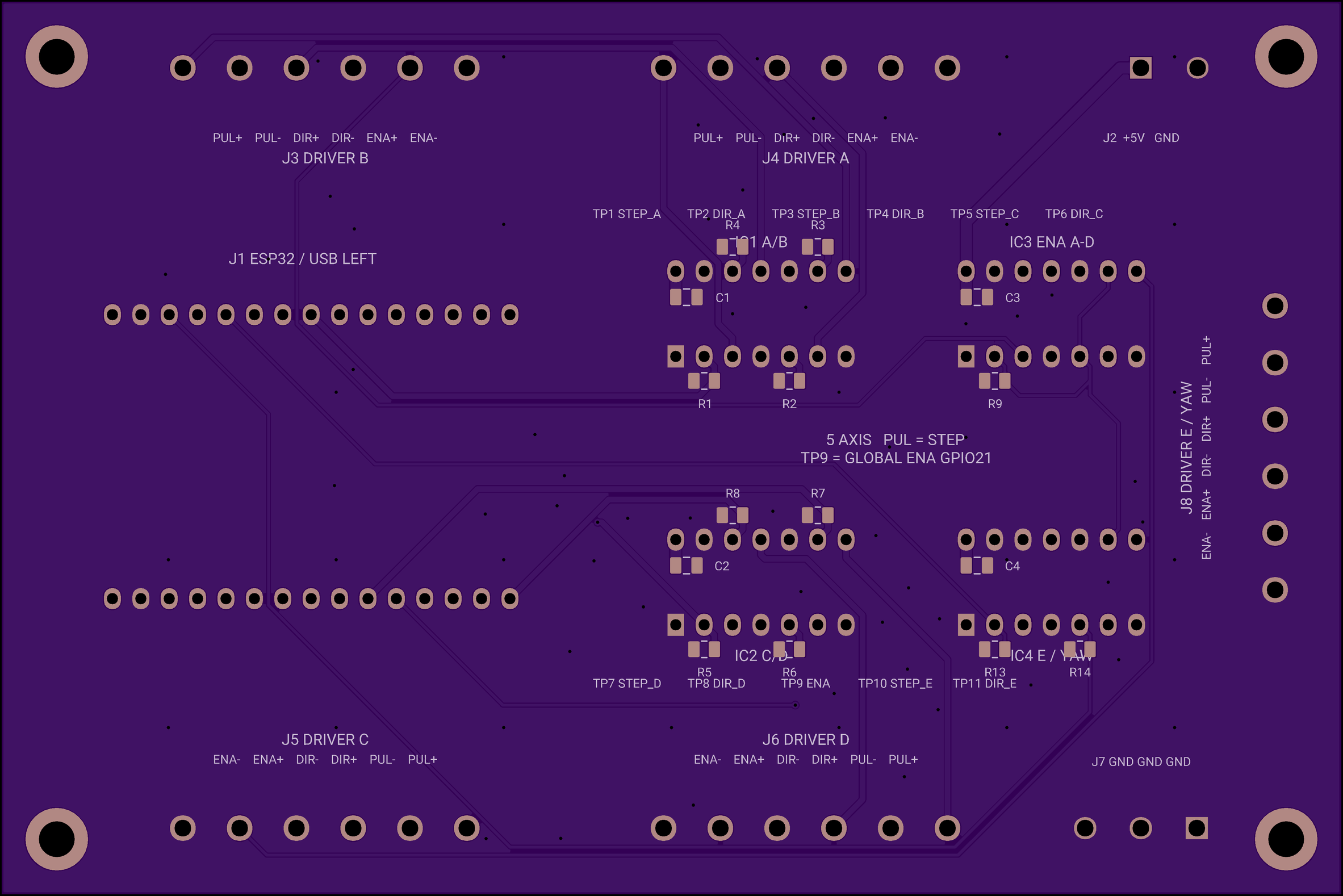
Buffer channels — which channel carries which signal
| Chip | Ch | In | Out | Signal | Goes to | In ✓ | Out ✓ |
|---|---|---|---|---|---|---|---|
| IC1 | 1 | 2 | 3 | STEP_A · GPIO 25 | J4 PUL+ | ☐ | ☐ |
| IC1 | 2 | 5 | 6 | DIR_A · GPIO 26 | J4 DIR+ | ☐ | ☐ |
| IC1 | 3 | 9 | 8 | STEP_B · GPIO 27 | J3 PUL+ | ☐ | ☐ |
| IC1 | 4 | 12 | 11 | DIR_B · GPIO 32 | J3 DIR+ | ☐ | ☐ |
| IC2 | 1 | 2 | 3 | STEP_C · GPIO 33 | J5 PUL+ | ☐ | ☐ |
| IC2 | 2 | 5 | 6 | DIR_C · GPIO 18 | J5 DIR+ | ☐ | ☐ |
| IC2 | 3 | 9 | 8 | STEP_D · GPIO 19 | J6 PUL+ | ☐ | ☐ |
| IC2 | 4 | 12 | 11 | DIR_D · GPIO 23 | J6 DIR+ | ☐ | ☐ |
| IC3 | 1 | 2 | 3 | ENABLE · GPIO 21 | J3 ENA+ | ☐ | ☐ |
| IC3 | 2 | 5 | 6 | ENABLE · GPIO 21 | J4 ENA+ | ☐ | ☐ |
| IC3 | 3 | 9 | 8 | ENABLE · GPIO 21 | J5 ENA+ | ☐ | ☐ |
| IC3 | 4 | 12 | 11 | ENABLE · GPIO 21 | J6 ENA+ | ☐ | ☐ |
| IC4 | 1 | 2 | 3 | STEP_E · GPIO 14 | J8 PUL+ | ☐ | ☐ |
| IC4 | 2 | 5 | 6 | DIR_E · GPIO 13 | J8 DIR+ | ☐ | ☐ |
| IC4 | 3 | 9 | 8 | ENABLE · GPIO 21 | J8 ENA+ | ☐ | ☐ |
| IC4 | 4 | 12 | 11 | tied to GND | no connection | ☐ | ☐ |
On all four chips OE pins 1, 4, 10 and 13 go to GND
(outputs permanently enabled — there is no tri-state on this board), pin 14 = 5V,
pin 7 = GND. IC3’s four inputs are all on the one ENABLE_IN net, which is the
design intent. IC4 channel 4 is a terminated spare — its input is tied to GND rather than left
floating, and its output goes nowhere. That is better practice than leaving it open.
J1 — all thirty pads
⚠️ Counting convention, stated once so it cannot drift: the silkscreen says
J1 ESP32 / USB LEFT, so position 1 is the LEFTMOST pad, at the USB end, counting
left → right in each row. Upper and lower rows, not columns.
| UPPER row (the DevKit’s VIN side) | |||
|---|---|---|---|
| Pos | DevKit | Net | GPIO |
| 1 | VIN | 5V | — |
| 2 | GND | GND | — |
| 3 | 13 | DIR_E | GPIO 13 |
| 4 | 12 | — not connected — | — |
| 5 | 14 | STEP_E | GPIO 14 |
| 6 | 27 | STEP_B | GPIO 27 |
| 7 | 26 | DIR_A | GPIO 26 |
| 8 | 25 | STEP_A | GPIO 25 |
| 9 | 33 | STEP_C | GPIO 33 |
| 10 | 32 | DIR_B | GPIO 32 |
| 11 | 35 | — not connected — | — |
| 12 | 34 | — not connected — | — |
| 13 | VN | — not connected — | — |
| 14 | VP | — not connected — | — |
| 15 | EN | — not connected — | — |
| LOWER row (the DevKit’s 3V3 side) | |||
|---|---|---|---|
| Pos | DevKit | Net | GPIO |
| 1 | 3V3 | — not connected — | — |
| 2 | GND | GND | — |
| 3 | 15 | — not connected — | — |
| 4 | 2 | — not connected — | — |
| 5 | 4 | — not connected — | — |
| 6 | RX2 | — not connected — | — |
| 7 | TX2 | — not connected — | — |
| 8 | 5 | — not connected — | — |
| 9 | 18 | DIR_C | GPIO 18 |
| 10 | 19 | STEP_D | GPIO 19 |
| 11 | 21 | ENABLE | GPIO 21 |
| 12 | RX0 | — not connected — | — |
| 13 | TX0 | — not connected — | — |
| 14 | 22 | — not connected — | — |
| 15 | 23 | DIR_D | GPIO 23 |
- The silkscreen says
USB LEFT. - The netlist puts 5V at upper position 1 and GND at position 2 of both rows — and VIN / 3V3 are the USB-end pins on a 30-pin DevKit.
- The full thirty-pad sequence matches the stock DOIT V1 pinout exactly, in order, including every unused pin — VIN, GND, 13, 12, 14, 27, 26, 25, 33, 32, 35, 34, VN, VP, EN on the upper row and 3V3, GND, 15, 2, 4, RX2, TX2, 5, 18, 19, 21, RX0, TX0, 22, 23 on the lower.
★ Verify the bare board first — before any part is soldered
Do this on a bare board, cold, with nothing fitted. Every pad is reachable from both sides, nothing is in the way, and continuity means what it says because there is no semiconductor anywhere in the path. You have three boards — keep one permanently bare as the tracer. That is what made the v1.0 verification possible without disturbing a working assembly.
The method, per channel. An SN74AHCT125 is four independent buffers.
Socket input pad → J1 gives you which ESP32 pin drives it.
Socket output pad → screw terminal gives you which signal it becomes.
Counting the socket pins on THIS board — verified 2026-09-17 from the Gerbers, not the render:
each socket has exactly one rectangular pad (aperture D16, 1.5 × 2.0 mm)
and thirteen ovals; 4 squares and 52 ovals board-wide, which is 14 × 4 with no exceptions.
That square pad is pin 1. All four sit at the bottom-left, and the chips run
horizontally (pads span 15.24 mm in X, rows 7.62 mm apart). So:
the notch faces LEFT, pin 1 is bottom-left, count 1→7 rightward along the bottom row, then
8→14 leftward along the top row.
⚠ An earlier draft of this page said “notch at the top, pin 1 top-left, count down the left”
— that is the vertical orientation and is wrong for this board. It would have you counting the wrong
way around the socket, which is exactly how v1.0 ended up 2-of-8 wrong. Confirm every beep by lifting a probe and hearing it stop — a probe tip
bridging two adjacent pads gives a false hit, and that is what caused the pad 18-vs-19 mix-up on v1.0.
| Chip | Ch | In | Out | Chip’s signal set | Input traces to… | Output traces to… |
|---|---|---|---|---|---|---|
| IC1 | 1 | 2 | 3 | STEP A · DIR A · STEP B · DIR B → J4 PUL+ / DIR+ · J3 PUL+ / DIR+ | ☐ J1 pad ____ = GPIO ____ | ☐ ____________ |
| IC1 | 2 | 5 | 6 | ☐ J1 pad ____ = GPIO ____ | ☐ ____________ | |
| IC1 | 3 | 9 | 8 | ☐ J1 pad ____ = GPIO ____ | ☐ ____________ | |
| IC1 | 4 | 12 | 11 | ☐ J1 pad ____ = GPIO ____ | ☐ ____________ | |
| IC2 | 1 | 2 | 3 | STEP C · DIR C · STEP D · DIR D → J5 PUL+ / DIR+ · J6 PUL+ / DIR+ | ☐ J1 pad ____ = GPIO ____ | ☐ ____________ |
| IC2 | 2 | 5 | 6 | ☐ J1 pad ____ = GPIO ____ | ☐ ____________ | |
| IC2 | 3 | 9 | 8 | ☐ J1 pad ____ = GPIO ____ | ☐ ____________ | |
| IC2 | 4 | 12 | 11 | ☐ J1 pad ____ = GPIO ____ | ☐ ____________ | |
| IC3 | 1 | 2 | 3 | GPIO21 ENA — all four → ENA+ on J3, J4, J5, J6 | ☐ J1 pad ____ = GPIO ____ | ☐ ____________ |
| IC3 | 2 | 5 | 6 | ☐ J1 pad ____ = GPIO ____ | ☐ ____________ | |
| IC3 | 3 | 9 | 8 | ☐ J1 pad ____ = GPIO ____ | ☐ ____________ | |
| IC3 | 4 | 12 | 11 | ☐ J1 pad ____ = GPIO ____ | ☐ ____________ | |
| IC4 | 1 | 2 | 3 | STEP E · DIR E · GPIO21 ENA · 1 spare → J8 PUL+ / DIR+ / ENA+ · 1 unused | ☐ J1 pad ____ = GPIO ____ | ☐ ____________ |
| IC4 | 2 | 5 | 6 | ☐ J1 pad ____ = GPIO ____ | ☐ ____________ | |
| IC4 | 3 | 9 | 8 | ☐ J1 pad ____ = GPIO ____ | ☐ ____________ | |
| IC4 | 4 | 12 | 11 | ☐ J1 pad ____ = GPIO ____ | ☐ ____________ |
Fifteen live channels, two readings each. Which channel of a chip carries which signal is deliberately left blank — that is the answer the tracing produces, not an input to it. The design fixes only which chip handles which pair of axes; the router chose the channels, and the only place that is written down is the copper. Fill the last two columns in and they become the pin map. The four IC3 inputs should all land on the same J1 pad, GPIO 21 — that is correct and is the point of the design, one pin disabling every axis. IC4 channel 4 is unused.
⚠ Orientation — check before soldering J1
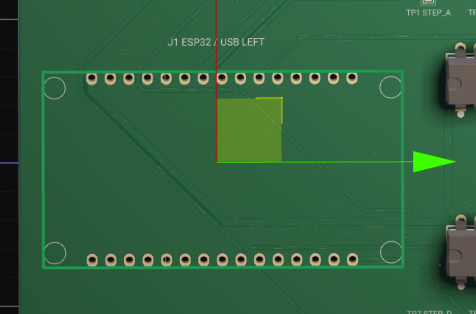
The socket takes the ESP32 either way round, and every pin is wrong if it is reversed. J1's thirty pads are identical ovals with no pin-1 marker — each chip got a square pad at pin 1, J2 and J7 got one, J1 did not. And the module covers that silkscreen once seated, so read it before the board disappears underneath.
Three checks, in this order. The module is never exposed until the first two pass.
- Continuity — nothing powered, no module. Buzz from J7 to find J1's ground pad, and from J2's +5V
to find its supply pad. On a 30-pin DevKit, GND and VIN are adjacent, at positions 14 and 15 of the left
column, so finding the board's two power pads side by side confirms you have the right end.
⚠ Adjacency survives a flip — check the order too. VIN sits closer to the USB end than GND. So the 5V pad should be nearer the left edge, with ground one position further in. Reversed means the module would go in backwards.
⚠ GND is not unique: a 30-pin DevKit has GND at position 14 in both columns, plus 3V3 at the bottom right. A single ground beep can mislead if you lose track of which column you are on — which is exactly why you check 5V as well. - 5 V into J2 — still no module. J1's supply pad is on the same net, so it goes live. Walk a voltmeter across J1: one pad reads 5 V, one reads 0, the other twenty-eight read nothing. That finds both power pads with a meter rather than a beeper, and nothing is at risk with an empty socket.
- Seat the module, then read 3V3. Its 3V3 pin should sit at 3.3 V. This is the good final confirmation precisely because you did not wire it — it comes from the module's own regulator, so seeing it means the supply reached the correct pin.
Verification record
Checked three independent ways before ordering, deliberately not trusting any single view of the design:
| Method | Found |
|---|---|
| Drill-coordinate parse | J1 rows 25.4 mm, pitch 2.54, span 35.56, drills 1.0 mm; all seven terminals 1.5 mm; board 120.00 × 80.00 |
| IPC-D-356 netlist parse | R1–R11 each on its own isolated net; C1–C4 across 5V/GND; no merged STEP/DIR nets; ENA reaching IC3 ×4 and IC4 ×1 |
| OSH Park render | Independent rendering by different software — passives on the underside, all footprints present |
317 records, missing the 327 continuation records where
the passives live, which produced a false alarm.
Only the exported manufacturing data is authoritative, and it has to be parsed completely.
Same failure mode as v1.0's J11 ground bus: a note saying "connected, confirmed by continuity" when the continuity
had only ever been hole-to-hole.
Order
| Fab | OSH Park — Lake Oswego, OR |
|---|---|
| Order | fB58RrsE, 2026-09-17 |
| Spec | 120 × 80 mm, 2 layer, standard 1.6 mm, 1 oz |
| Cost | $74.40 for 3, free shipping |
| Gerbers | ~/earthquake-sim/hardware/ss_stepper_board_v1_1/gerbers/ — the 858ca36c… package (08:14 export) is the one accepted |